Gerhard Fasol gave a talk at the Rotary Club Stuttgart-Solitude on Monday, September 6th, 1999, 18:30pm
Topic: “New Business Opportunities in Japan – the world’s second largest market”
(Audience: CEOs, Managers, VPs, of Stuttgart area companies)
Gerhard Fasol gave a talk at the Rotary Club Stuttgart-Solitude on Monday, September 6th, 1999, 18:30pm
Topic: “New Business Opportunities in Japan – the world’s second largest market”
(Audience: CEOs, Managers, VPs, of Stuttgart area companies)
Gerhard Fasol gave a talk at the German Chamber of Commerce in Tokyo (Deutsche Industrie und Handelskammer in Japan) on Thursday, March 18, 1999, at 18:00pm followed by a buffet reception to continue the discussions.
Topic: “Trends in Japan’s R&D World and their Effects on Foreign Corporations”
(Audience: managers of Japan subsidiaries of German multinationals: e.g. BOSCH, VW, Porsche, Siemens etc.)
Gerhard Fasol gave a presentation at the Conference on “Intellectual Property in an Era of Intellectual Renaissance” Awashima-Hotel (Japan) organized by Keio-University at the Awashima-Hotal on Awashima-Island, on January 29-31, 1999.
Title: Creativity, Intellectual Property and Entrepreneurs in Japan: Some Comments and Observations
Participants: approx. 55 CEOs, Chairmen, Vice-Presidents of major Japanese and US corporations, President of Japan’s Patent Office, former Presidents of the US Patent Office, US Embassador…
Gerhard Fasol gave an evening Colloquium talk at the beautiful Magnus-Haus in the center of Berlin, Germany, on Tuesday, December 1st, 1998 at 19:30. The talk was followed by a buffet reception, where we continued discussions until late at night.
Title: “Crisis and opportunities in Japan’s Research and Development World – an entrepreneurs perspective”
(Audience: Presidents, high-level managers of German national and industrial R&D laboratories, Berlin area researchers, managers, and Professors)
Gerhard Fasol gave a talk at the Department of Electrical Engineering of Princeton University, on Monday April, 4, 1998, at 4:00pm.
Title: “Recent Development in Blue Laser and Nanoscale Materials”
Gerhard Fasol was one of the invited speakers of the “Device Applications of Nanoscale Materials Symposium” at the 1998 National ACS Meeting in Dallas, Texas, which was organized by John St. John of Texas Christian University.
Gerhard Fasol’s talk: “Selective Electrodeposition of Magnetic and Metallic Nanowires: A New Approach to a Fundamental Technology”
Symposium purpose:
The two main purposes of this symposium are (1) to demonstrate current, innovative applications of chemistry in the nanometer size regime for use in optoelectronics and (2) to identify potential areas for partnerships between industry and academia where research in nanoscale chemistry can be applied to emerging technologies. It is hoped that this symposium will benefit chemists working in nanotechnology by providing a forum for discussing applications with leading industries.
Press Conference participants:
Technical program
For Gerhard Fasol’s related publications see:
Copyrigh (c) 2013 Eurotechnology Japan KK All Rights Reserved
After Masaru Ibuka (井深大) died on December 19, 1997, NATURE asked me to write an obituary about Masaru Ibuka, which was published in Nature on February 26, 1998, and you can download the article as a pdf-file here. The reference is: Gerhard Fasol, “Obituary: Masaru Ibuka (1908-97)”, Nature 391, p. 848 (26 February 1998).
I used several weeks of my spare time to research and write this obituary. For example, I worked to reach and talk with several people who had met Ibuka in person, since I had never personally met Ibuka. As another example: General McArthur’s Government of Japan wanted to communicate with the population of Japan via radio, however, radio receiver production in Japan was very inefficient at that time due to quality problems, leading to very low yield. So General McArthur’s Government brought Quality experts Homer Sarasohn and Charles Protzmann to Japan to teach classes in quality management. I found out that Ibuka was a keen student of these quality classes. To understand this better, I phoned with a retired officer of General McArthur’s Government, and I also found relatives of Homer Sarasohn, who very kindly gave me a lot of information about Homer Sarasohn’s work in teaching quality management in Japan.
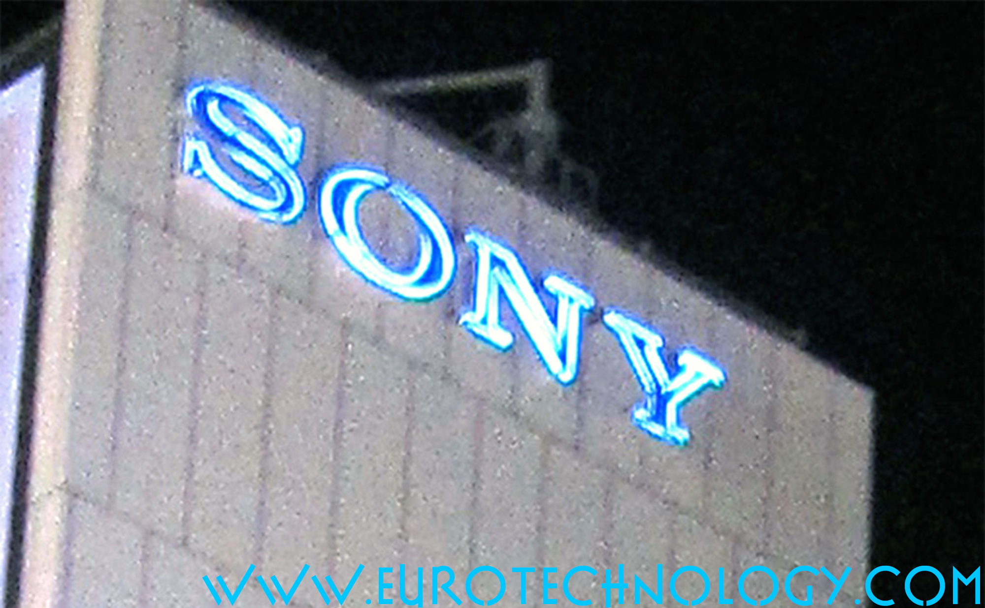
Interestingly, there is a lot of misunderstandings and myths around SONY, some of which I clarified in the Nature obituary for Masaru Ibuka.
Reality: SONY was founded as Tokyo Tsushin Kenkyusho (the Tokyo Communications Laboratory) by Masaru Ibuka and by Akio Morita, who are the two co-founders of Tokyo Tsushin Kenkyusho, the company name was later changed to SONY.
Reality: SONY is a Japanese company with headquarters in Tokyo-Shinagawa. The reason why many people think that SONY is an American company, is that SONY’s company name and brand name in Japan is written in Katakana, while traditional Japanese companies always write their company in Chinese characters (Kanji). (Note however, that Nissan President Carlos Ghosn, says that companies have no nationality).
Reality: Leo Esaki discovered the tunnel diode as a researcher at Tokyo Tsushin Kenkyusho, which later changed the company name to SONY. Leo Esaki then moved to IBM Yorktown Heights R&D labs, and was awarded the Nobel Prize while working at IBM for his discovery of the tunnel diode, which he discovered while working at Tokyo Tsushin Kenkyusho.
More about SONY and Japan’s electronic companies in our Report on Japan’s electronics industry.
Copyright (c) 1996-2014 Eurotechnology Japan KK All Rights Reserved
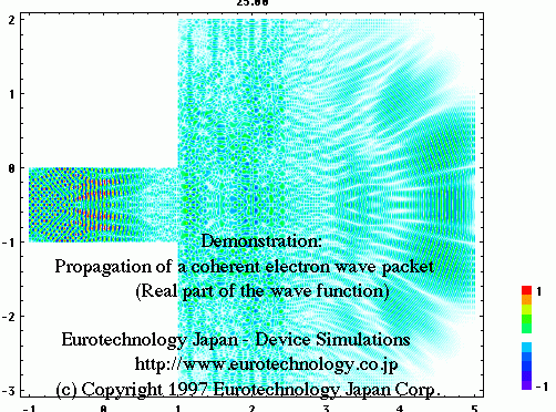
Conference presentation by Gerhard Fasol at the 5th International Workshop on Femtosecond Technology FST’98, Tsukuba, Japan, February 12-13, 1998, on
“Simulation and Visualization of the Dynamics of Electron Wave Packets on a Femto-Second Time-Scale”
Details of our work on the simulation and visualization of electron wave packet motion.